Philips DVDR3355 Service Manual
Dvd-video recorder
Hide thumbs
Also See for DVDR3355:
- User manual (62 pages) ,
- Technical specifications (2 pages) ,
- Firmware upgrade manual (2 pages)
Table of Contents
Advertisement
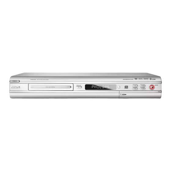
DVD-Video Recorder
CLASS 1
LASER PRODUCT
Contents
1
2
3
4
5
6
7
© Copyright 2005 Philips Consumer Electronics B.V. Eindhoven, The Netherlands.
All rights reserved. No part of this publication may be reproduced, stored in a
retrieval system or transmitted, in any form or by any means, electronic,
mechanical, photocopying, or otherwise without the prior permission of Philips.
Published by KC-TE 0519 AV Systems
Version 1.1
DVDR3355/37/55 & DVDR3365/75/97
Contents
Page
2
4
6
8
11
19
19
20
21
22
23
24
8
25
26
26
27
28
29
9
30
31
32
33
34
35
40
Printed in the Netherlands
DVDR3355 & DVDR3365
Subject to modifi cation
Page
41
42
42
43
43
43
44
45
46
47
48
49
50
51
51
51
56
59
59
64
75
75
76
81
EN 3139 785 30981
Advertisement
Table of Contents

Related Manuals for Philips DVDR3355


Summary of Contents for Philips DVDR3355
-
Page 1: Table Of Contents
Layout: Analog-Main Part (Bottom View) Front: Front Panel - Display © Copyright 2005 Philips Consumer Electronics B.V. Eindhoven, The Netherlands. All rights reserved. No part of this publication may be reproduced, stored in a retrieval system or transmitted, in any form or by any means, electronic, mechanical, photocopying, or otherwise without the prior permission of Philips. -
Page 2: Technical Specifi Cations And Connection Facilities
Channel 25 / 503,25 MHz, Test pattern: standard test pattern. Test equipment: Fluke 54200 TV Signal generator RF Level 74dBμV Test streams: Philips Standard test pattern Measured on Cinch Out Frequency response : 0.1 - 3.58 MHz -1 ± 3dB 1.3.1... -
Page 3: Digital Output
Technical Specifi cations and Connection Facilities 3139 785 30981 EN 3 Analogue Inputs / Outputs Audio Performance CD 1.4.1 External In (Rear) 1.6.1 Cinch Output Rear Output voltage 2 channel mode : 2Vrms ± 1dB Video - Y/C (Hosiden) according IEC 933-5 Channel unbalance (1kHz) : <1dB Superimposed DC-level on pin 4 (load ≥... -
Page 4: Safety Information, General Notes & Lead Free Requirements
EN 4 3139 785 30981 Safety Information, General Notes & Lead Free Requirements Safety Information, General Notes & Lead Free Requirements Safety Instructions Warnings 2.1.1 General Safety 2.2.1 General Safety regulations require that during a repair: • All ICs and many other semiconductors are susceptible to •... - Page 5 “Video Plus+” and “PlusCode” are registered trademarks of workshop during a repair: the Gemstar Development Corporation. The “Video Plus+” • Use only lead-free solder alloy Philips SAC305 with order system is manufactured under licence from the Gemstar Development Corporation. code 0622 149 00106. If lead-free solder-pate is required, please contact the manufacturer of your solder-equipment.
-
Page 6: Directions For Use
Directions For Use The following except of the Quick Use Guide serves as an introduction to the set. The Complete Direction for the Use can be downloaded in different languages from the internet site of Philips Customer care Center: www.p4c.philips.com... -
Page 7: Start Playback
Connect the AUDIO L/R (red/white) jacks at the back of the DVD recorder to the correspond AUDIO input jacks on a TV, stereo system or receiver. Turn on the connected system and select the appropriate channel. NEED HELP? Read the accompanying User Manual or visit our website www.philips.com/support... -
Page 8: Mechanical Instructions
EN 8 3139 785 30981 Mechanical Instructions Mechanical Instructions Dismantling and Assembly of the Set 4.1.2 Dismantling of the Front Panel Assembly 1) Remove the 3 screws 188 and release the 2 snap hooks For item numbers please see the exploded view in Chapter 9. on the side before removing the front assembly. - Page 9 Mechanical Instructions 3139 785 30981 EN 9 4.1.3 Dismantling of the Basic Engine 4.1.4 Dismantling of the Digital Board 1) Remove the Cover Tray (See 4.1.1). 1) Remove the 4 screws 272 to loose the Digital Board as shown in Figure 4-7. 2) Remove the 4 screws 260 to free the Basic Engine.
- Page 10 EN 10 3139 785 30981 Mechanical Instructions 4.1.5 Dismantling of the Analog Board 1) Remove 5 screws 244 and 4 screws 252 and screw 230. 2) Remove 4 screws 270 and 3 screws 268. 3) Service Position can be achieved by fl ipping the analog board to the Vertical Position as shown in Figure 4-9.
-
Page 11: Upgrade Software & Repair Chart
7. Remove the Upgrade Disc and press OK button to confi rm 8. The TV screen goes blank, tray close and after a while the Philips Logo screen appear again. C. How to read out the fi rmware version to confi rm upgrading 1. - Page 12 EN 12 Upgrade Software & Repair Chart 3139 785 30981 Repair Chart 5.2.1 Completely Dead Set Check primary fuse Holder 1401 Check Voltage at Fuse 1405,1406,1407,1408,1409,1410 Check Voltage at F424,F434,F406,F439,F409,F447,F449,F457 Check STBY at F441=high? Measure Voltage across F420 & F459 Check DRAIN (pin 8) at F417 = 300V ? Check waveform at F417, I407, I409...
- Page 13 Upgrade Software & Repair Chart 3139 785 30981 EN 13 5.2.2 Cannot Read Disk Check cable connection: Supply cable from Analog 1404 to Drive 1600 (4 pin) Check cable connection: Analog 1571 to Drive 1600 (40 pin) Check Voltage at analog board F415 = 12V F416 = 5V Check Fuse I406...
- Page 14 EN 14 Upgrade Software & Repair Chart 3139 785 30981 5.2.4 Audio No Sound (Playback) Check Test Point I603, I604, I605, I609 = square pulse Check Test Point I613 = 11.2V –12V I624 = 3.3V I615 = high Monitor Test Point I618 &...
- Page 15 Upgrade Software & Repair Chart 3139 785 30981 EN 15 5.2.5 Audio No Sound (TV & External Source) Part 1 Check I316 & I319 = sine wave Replace the component in between these 2 & test point (Op Amp 7300) Check I606 &...
- Page 16 EN 16 Upgrade Software & Repair Chart 3139 785 30981 5.2.6 No Video Out Upon Power ON (Assume set is not dead) Check Digital Board Waveform at CVBS T524 Replace Digital Board If no Waveform T522 T523 T520 T518 T521 Check Cable Connection on Analog Board Check Test point for Waveform CVBS...
- Page 17 Upgrade Software & Repair Chart 3139 785 30981 EN 17 5.2.7 No Video In Only Check Supply on digital board Check Clock At Replace Crystal 1461 T432 & T461 = 14.318MHz Check Video Input Check respective i/p test point T524, T526, T527, T528, T529, T530, T531, of video in at analog board T532 T533 T535 Replace VIP (7401) IC...
- Page 18 EN 18 Upgrade Software & Repair Chart 3139 785 30981 Notes:...
-
Page 19: Block Diagrams,Waveforms, Wiring Diagram
Block Diagrams, Waveforms, Wiring Diagram. 3139 785 30981 EN 19 Block Diagrams, Waveforms, Wiring Diagram Overall Block Diagram of the Set Front Keyboards ANALOG BOARD 1201 CONTROL LINES, AND SUPPLY LINES CONTROL LINES 1922 AFCRI AFCLI CVBSFIN AUDIO L CONTROL UNIT SLAVE CFIN MICROPROCESSOR YFIN... -
Page 20: Control Block Diagram
Block Diagrams, Waveforms, Wiring Diagram. 3139 785 30981 EN 20 Control Block Diagram Control Block Diagram Analog Board Fr ont Fa n FAN_CTRL Ke ys I2 C I2C Bu s ASP Analog Sl av e Processo r Repeater 3V 3 NEC uPD-16316GBT IN T AF C... -
Page 21: Wiring Diagram
Block Diagrams, Waveforms, Wiring Diagram. 3139 785 30981 EN 21 Wiring Diagram Interconnection Diagram Architecture DVDR3355 V1.0 Kek YH 06.01.2005 FRONT PCB MAINS KB_FC KB_FC CORD 1600 1800 1205 1206 1803 1804 1201 MAINS P A_YG FAN_P MAINS L SCL0... -
Page 22: Waveforms Of Analog Board
Block Diagrams, Waveforms, Wiring Diagram. 3139 785 30981 EN 22 Waveforms Waveforms of Analog Board F219 Y_OUT F220 C_OUT F222 CVBS_OUT F236 C_OUT F237 Y_OUT F238 D_VR F239 D_YG F240 D_UB F417 VDrain (No Disc) F417 Vdrain(Standby) I300 & I301 AIN2R & AIN2L I302 &... -
Page 23: Waveforms Of Digital Board
Block Diagrams, Waveforms, Wiring Diagram. 3139 785 30981 EN 23 Waveforms of Digital Board IC 7211 PIN 45 IC 7211 PIN 46 IC 7401 PIN74 IC 7401 PIN75 T121 T525, T526,T529 T527,T531,T535 SY_RE,SY_FR, CY T122 T351 IC7301 PIN 42 T352 IC 7301 PIN 43 CVBS_TU, CVBS_RE,CVBS_FR T528,T530 SC_RE, SC_FR T532 BPr... -
Page 24: Test Point Overview For Analog Board
Block Diagrams, Waveforms, Wiring Diagram. 3139 785 30981 EN 24 Test Points Overview for Analog Board AnalogBd_TestPoint_31916.pdf 2005-09-07... -
Page 25: Test Point Overview For Digital Board
Block Diagrams, Waveforms, Wiring Diagram. 3139 785 30981 EN 25 Test Points Overview for Digital Board 3355 Testpoint-digital-31873.pdf 2005-04-01... -
Page 26: Circuit Diagram And Pwb Layout
Circuit Diagrams and PWB Layouts 3139 785 30981 EN 26 Circuit Diagrams and PWB Layouts Analog: Frontend Video (FV) 0803 H1 I119 C5 1100 F1 1101 C1 2100 B6 2101 B12 from PS 2102 F5 2103 F6 5VSTBY 33VSTBY 2104 F7 2105 H4 2106 H4 5V_FV... -
Page 27: Analog: Video In / Out (Iov)
Circuit Diagrams and PWB Layouts 3139 785 30981 EN 27 Analog: Video In / Out (IOV) 1201-1 I13 7202 D10 1201-3 C13 7203 E12 1202 E2 7204 F12 1203 F14 7205 H12 1204 H2 F200 A6 1205 I7 F201 C3 1206 I7 F202 C3 1207-1 C2... -
Page 28: Analog: Audio In / Out (Ioa)
Circuit Diagrams and PWB Layouts 3139 785 30981 EN 28 Analog: Audio In / Out (IOA) 1201-2 E9 I318 C8 1207-2 A1 I319 C8 2113 A2 I320 D8 2300 A3 I321 D8 2302 B3 2303 B2 REAR IN 1 2304 C2 2305 C2 2306 A5 F300... -
Page 29: Analog: Power Supply (Ps)
Circuit Diagrams and PWB Layouts 3139 785 30981 EN 29 Analog: Power Supply (PS) 1400 C1 3466 D12 F435 D8 1401 B1 3467 D12 F436 D8 1402 B3 3468 F7 F438 D12 1403 D1 3469 G7 F439 D13 1404 G1 3470 F9 F441 D13 F423... -
Page 30: Analog: Multi Sound Processing (Msp)
Circuit Diagrams and PWB Layouts 3139 785 30981 EN 30 Analog: Multi Sound Processing (MSP) 1500 F6 2500 A1 2501 C1 2502 C1 from PS 8VSTBY 2503 E2 8VSTBY 2504 E2 2505 A5 2506 A5 2507 A6 2508 A6 2509 A7 I512 I513 2510 B8... -
Page 31: Analog: Audio Converter (Dac_Adc)
Circuit Diagrams and PWB Layouts 3139 785 30981 EN 31 Analog: Audio Converter (DAC_ADC) 1600 C1 F605 D1 2600 B1 F606 D2 2603 D3 F607 D1 2604 D3 F608 D1 2605 D4 F609 D1 2606 D4 F610 D1 2607 E1 F611 E1 5VSTBY 2608 E1... -
Page 32: Analog: Digital In / Out 1 (Digio 1)
Circuit Diagrams and PWB Layouts 3139 785 30981 EN 32 Analog: Digital In / Out 1 (DigiO 1) 0006 F2 1700 C9 1701 D9 2700 A4 2701 A4 2702 D2 2703 E5 2704 D5 2705 D8 2706 D7 I712 2707 F8 3700 A3 3701 A4 3702 B4... -
Page 33: Analog: Control Unit (Cu)
Circuit Diagrams and PWB Layouts 3139 785 30981 EN 33 Analog: Control Unit (CU) 0005 E1 1800 C1 1802 A3 1803 B3 1804 E4 2800 E3 3800 D1 3801 E1 3802 E2 3803 E2 frm/to Dig Board 3804 F2 3805 E3 HLW20S-2C7 3806 E3 3807 F3... -
Page 34: Layout: Analog-Main Part (Top View)
Circuit Diagrams and PWB Layouts 3139 785 30981 EN 34 Layout: Analog-Main Part (Top View) AnalogBd_3139_243_31916_TopView.pdf 2005-09-07... -
Page 35: Layout: Analog-Main Part (Bottom View)
Circuit Diagrams and PWB Layouts 3139 785 30981 EN 35 Layout: Analog-Main Part (Bottom View) Part 1 Part 2 AnalogBd_3139_243_ AnalogBd_3139_243_ 31916_BottomView_a 31916_BottomView_b Part 3 Part 4 AnalogBd_3139_243_ AnalogBd_3139_243_ 31916_BottomView_c 31916_BottomView_d AnalogBd_3139_243_31916_BottomView.pdf 2005-09-07... - Page 36 Circuit Diagrams and PWB Layouts 3139 785 30981 EN 36 Layout: Analog-Main Part (Bottom View) Part 1 AnalogBd_3139_243_31916_BottomView.pdf 2005-09-07...
- Page 37 Circuit Diagrams and PWB Layouts 3139 785 30981 EN 37 Layout: Analog-Main Part (Bottom View) Part 2 AnalogBd_3139_243_31916_BottomView.pdf 2005-09-07...
- Page 38 Circuit Diagrams and PWB Layouts 3139 785 30981 EN 38 Layout: Analog-Main Part (Bottom View) Part 3 AnalogBd_3139_243_31916_BottomView.pdf 2005-09-07...
- Page 39 Circuit Diagrams and PWB Layouts 3139 785 30981 EN 39 Layout: Analog-Main Part (Bottom View) Part 4 AnalogBd_3139_243_31916_BottomView.pdf 2005-09-07...
-
Page 40: Front: Front Panel - Display
Circuit Diagrams and PWB Layouts 3139 785 30981 EN 40 Front: Front Panel - Display 0100 E3 4101 I4 I107 A4 1100 E10 4102 F1 I108 A4 1101 F10 4103 E1 12VSTBY 1203 1102 H1 4104 D2 HUV-08SS65T 1201 F13 4109 H11 I103 3104... -
Page 41: Front: Front Panel - Audio/Video In
Circuit Diagrams and PWB Layouts 3139 785 30981 EN 41 Front: Front Panel - Audio/Video-In 1202 B1 1300 C3 1301 D1 1401 E1 1402 E3 3200 5VSTBY 5ESD 2200 A1 2201 A2 2202 A2 2203 A3 2204 B1 2205 D2 2206 D2 2207 B2 5ESD... -
Page 42: Layout: Front Panel (Top Copper Pattern)
Circuit Diagrams and PWB Layouts 3139 785 30981 EN 42 Layout: Front Panel (Top Copper Pattern) - SMD + Components FrontPanel_Topview_31947_3355.eps 2005-04-01 Layout: Front Panel (Bottom Copper Pattern) - Components FrontPanel_Bottomview_31947_3355.eps 2005-04-01... -
Page 43: Front: Standby
Circuit Diagrams and PWB Layouts 3139 785 30981 EN 43 Front: Standby Layout: Standby (Top View) Layout: Standby (Bottom View) 1302 C2 1303 C4 2300 D2 6300 D2 6301 D3 F300 C2 F301 C2 I300 C4 1302 1303 I300 F300 EVQ11L05R S2B-EH F301... -
Page 44: Digital: Back-End Processor
Circuit Diagrams and PWB Layouts 3139 785 30981 EN 44 Digital: Back-End Processor 1101 B10 3176-4 H2 1111 E10 3177-1 I2 2101 B10 3177-2 I2 2102 B11 3177-3 I2 2105 G12 3177-4 I2 2108 F1 3178-1 I2 Back-end Flash (BEF) Communication (COM) 2109 F2 3178-2 I2... -
Page 45: Digital: Memory
Circuit Diagrams and PWB Layouts 3139 785 30981 EN 45 Digital: Memory 2201 D1 3277-2 F12 2202 D2 3277-3 F12 2203 D3 3277-4 F12 2204 D4 3281-1 F12 2205 D3 3281-2 F12 2211 B5 3281-3 F12 Memory 2212 B5 3281-4 F12 2213 B5 3283 G12 2214 B5... -
Page 46: Digital: Ieee 1394 Physical Layer
Circuit Diagrams and PWB Layouts 3139 785 30981 EN 46 Digital: IEEE 1394 Physical Layer 1351 C2 2301 B2 2302 C2 2303 C2 2304 C2 2305 C3 IEEE1394 Physical Layer 2306 C3 2307 C3 2321 F2 2341 E5 2343 E6 2351 C1 2352 C1 2361 D2... -
Page 47: Digital: Video Input Processor
Circuit Diagrams and PWB Layouts 3139 785 30981 EN 47 Digital: Video Input Processor 1461 A6 4474 C5 2401 A1 4475 C5 2402 A1 4476 C5 2403 A1 4477 C5 2404 A1 4478 C5 2411 B1 4479 C5 Video Input Processor 2412 B1 4480 E5 2413 B1... -
Page 48: Digital: Interfaces
Circuit Diagrams and PWB Layouts 3139 785 30981 EN 48 Digital: Interfaces 1501 C1 3576-2 G2 T590 H1 1502 H9 3576-3 G2 T591 H1 1511 H11 3576-4 G2 T592 H1 1512 H12 3577 G2 T593 H1 1521 A9 3578 G2 T594 H1 1522 A9 3579-1 H2... -
Page 49: Layout: Digital-Main Part (Top View)
Circuit Diagrams and PWB Layouts 3139 785 30981 EN 49 Layout: Digital-Main Part (Top View) 3355_Digital_hmc1_smc1_31874.pdf 2005-04-01... -
Page 50: Layout: Digital-Main Part (Bottom View)
Circuit Diagrams and PWB Layouts 3139 785 30981 EN 50 Layout: Digital-Main Part (Bottom View) 3355_Digital_smc2_31874.pdf 2005-04-01... -
Page 51: Circuit- And Ic Description
Circuit- and IC description 3139 785 30981 EN 51 Circuit- and IC description 8.1. Front Board (Panel – Display + Key) 8.2. Analog Board 8.1.1. General 8.2.1. General The pcba consist of the following parts: • This board consists of the following parts: Fan Control (OPTION) •... - Page 52 EN 52 3139 785 30981 Circuit- and IC Description 8.2.4. Tuner Frontend The Analog board supports 2 possible Tuner Frontend unit namely: • 1101 - PAL BG,DK and I Broadcast System • 1100 – NTSC-M Broadcast System It has a RF IN for antenna connection and RF OUT which provides a RF loop through for connection to the TV.
- Page 53 Circuit- and IC description 3139 785 30981 EN 53 8.2.5. Audio routing Figure 8-1 Analog Audio IO NAFTA...
- Page 54 EN 54 3139 785 30981 Circuit- and IC Description The sound processing is always done in stereo (that means separate left- and right- channel). Record path The complete selection of audio signal for recording is done by a HEF4052 [7301], which is a dual four-to-one mulitplexer. The input lines for the selector [7301] are coming either from MSP [7500] (AFEL/AFER) or cinch rear-in Ext 1 ( AIN1L/ AIN1R) or cinch rear-in Ext 2 (AIN2L/AIN2R) or the cinch...
- Page 55 Circuit- and IC description 3139 785 30981 EN 55 8.2.7. Video-routing Figure 8-2 Analog Video IO NAFTA...
-
Page 56: Digital Board
EN 56 3139 785 30981 Circuit- and IC Description 8.3. Digital Board The board encodes and multiplexes analogue video and The Digital Board is based on the highly integrated LSI ‘Domino’ BGA chip (Ball Grid Array), DMN-8602. This IC has digital uncompressed audio (I S) into an MPEG2 stream. - Page 57 Circuit- and IC description 3139 785 30981 EN 57 Video Part ATAPI connector 1571. The analogue video input signals CVBS, YC and RGB are It buffers the data streams that are coming from (or going to) routed via the board to connector 1521 and sent to Video the Basic Engine.
- Page 58 EN 58 3139 785 30981 Circuit- and IC Description 8.3.5. Power Supply • 2.5V supply for the SDRAM is generated by an ultra fast The Digital board is not powered in standby mode. The low dropout linear regulator [7515] control signal STBY on the analog board will enable the PSU •...
-
Page 59: Ic Description
Circuit- and IC description 3139 785 30981 EN 59 IC Description 8.4.1 Analog Board IC7421 - SMPS Control IC BLOCK DIAGRAM SUPPLY START-UP V CC DRAIN MANAGEMENT CURRENT SOURCE clamp internal UVLO start n.c. VALLEY supply M-level VOLTAGE CONTROLLED LOGIC OSCILLATOR 100 mV OVER-... - Page 60 EN 60 3139 785 30981 Circuit- and IC Description IC7500 - Multistand Sound Processor Family BLOCK DIAGRAM 23 24 28 32 ANA_IN+ DACM_L Loud- Pre- speaker processing Modulator sound ANA_IN- DACM_R proeessing I2S_DA_IN1 Loud- Pre- speaker I2S_DA_OUT processing sound I2S_DA_IN2 proeessing Source select...
- Page 61 Circuit- and IC description 3139 785 30981 EN 61 PIN CONFIGURATION VREF1 DACM_L SC1_OUT_R DACM_R SC1_OUT_L VREF2 AHVSUP 33 32 31 30 29 28 27 26 25 24 23 CAPL_M RESETQ AHVSS I2S_DA_IN2 AGNDC DVSS SC2_IN_L DVSUP SC2_IN_R ADR_CL MSP 34x5G I2S_DA_IN1 SC1_IN_L I2S_DA_OUT...
- Page 62 EN 62 3139 785 30981 Circuit- and IC Description PIN DESCRIPTION AND CONFIGURATION SDIN SCLK AMUTEC LRCK AOUTA MCLK VA_H AOUTB DIF1(SCL/CCLK) BMUTEC DIF0(SDA/CDIN) DEM(AD0/CS) VBIAS Pin Name Pin Description SDIN Serial Audio Data Input ( Input ) - Input for two’s complement serial audio data. SCLK Serial Clock ( Input ) - Serial clock for the serial audio interface.
- Page 63 Circuit- and IC description 3139 785 30981 EN 63 IC7606 - 96KHz Sampling 24-bit stereo audio ADC BLOCK DIAGRAM V DDA V SSA V RP V RN V ref SYSCLK V DDD UDA1361TS V SSD V INL ΣΔ MSSEL DECIMATION CLOCK FILTER CONTROL...
-
Page 64: Digital Board
EN 64 3139 785 30981 Circuit- and IC Description 8.4.2 Digital Board IC7301 - IEEE 1394a-2000 one port cable Transceiver/Arbiter BLOCK DIAGRAM Received Data Decoder/Retimer Link CNA † Interface SYSCLK LREQ TPA+ CTL0 TPA– CTL1 Cable Port TPB+ Arbitration and Control TPB–... - Page 65 Circuit- and IC description 3139 785 30981 EN 65 PIN CONFIGURATION PHP package terminal diagram PHP PACKAGE (TOP VIEW) 47 46 45 44 43 40 39 38 AGND SYSCLK CTL0 CTL1 AGND TPBIAS TSB41AB1 TPA+ TPA– TPB+ TPB– AGND 14 15 17 18 19 20 21 22 23 24 Figure 8-12...
- Page 66 EN 66 3139 785 30981 Circuit- and IC Description PIN DESCRIPTION TERMINAL TYPE TYPE DESCRIPTION DESCRIPTION NAME PHP NO. AGND 26, 32, 36 Supply – Analog circuit ground terminals. These terminals should be tied together to the low-impedance circuit board ground plane. AV DD 25, 35 Supply...
- Page 67 Circuit- and IC description 3139 785 30981 EN 67 TERMINAL TYPE TYPE DESCRIPTION DESCRIPTION NAME PHP NO. DGND 14, 46, 47 Supply – Digital circuit ground terminals. These terminals should be tied together to the low-impedance circuit board ground plane. DV DD 21, 44, 45 Supply...
- Page 68 EN 68 3139 785 30981 Circuit- and IC Description TERMINAL TYPE TYPE DESCRIPTION DESCRIPTION NAME PHP NO. PLLGND Supply – PLL circuit ground terminals. These terminals should be tied together to the low-impedance circuit board ground plane. PLLV DD Supply –...
- Page 69 Circuit- and IC description 3139 785 30981 EN 69 IC7401 - 4x10bit DigitalVideo Decoder with microvision BLOCK DIAGRAM Copy CVBS/Y/G Protection Data Detector Slicer Analog Front End VI_1_A Composite and S-Video Processor CVBS/ VI_1_B ADC1 Pb/B/C VI_1_C Luma CVBS/Y Separation Processing YCbCr 5-line...
- Page 70 EN 70 3139 785 30981 Circuit- and IC Description PIN DESCRIPTION TERMINAL DESCRIPTION DESCRIPTION NAME NUMBER Analog Video VI_1_A VI_1_x: Analog video input for CVBS/Pb/B/C VI_1_B VI_2_x: Analog video input for CVBS/Y/G VI_1_C VI_3_x: Analog video input for CVBS/Pr/R/C VI_2_A VI_4_A: Analog video input for CVBS/Y VI_2_B Up to 10 composite, 4 S-video, and 2 composite or 3 component video inputs (or a combination thereof)
- Page 71 Circuit- and IC description 3139 785 30981 EN 71 TERMINAL DESCRIPTION DESCRIPTION NAME NUMBER Host Interface I 2 C clock input I 2 C data bus Power Supplies AGND Analog ground. Connect to analog ground. A18GND_REF Analog 1.8-V return A18VDD_REF Analog power for reference 1.8 V CH1_A18GND CH2_A18GND...
- Page 72 EN 72 3139 785 30981 Circuit- and IC Description IC7501 - Power Distribution Switches BLOCK DIAGRAM Power Switch † Charge Pump Current Driver Limit UVLO Thermal Sense † Current Sense Figure 8-15 PIN CONFIGURATION TPS2041 D OR P PACKAGE (TOP VIEW) Figure 8-16...
- Page 73 Circuit- and IC description 3139 785 30981 EN 73 PIN DESCRIPTION TERMINAL DESCRIPTION DESCRIPTION NAME D OR P TPS2041 TPS2051 – Enable input. Logic low turns on power switch. – Enable input. Logic high turns on power switch. Ground 2, 3 2, 3 Input voltage Over current.
- Page 74 EN 74 3139 785 30981 Circuit- and IC Description IC7595 - Voltage Detector Series with Programmable Delay BLOCK DIAGRAM NCP303LSNxxT1 Open Drain Output Configuration Input Reset Output Figure 8-17 PIN DESCRIPTION AND CONFIGURATION PIN CONNECTIONS AND MARKING DIAGRAM Reset Output Input N.C.
-
Page 75: Exploded View & Spare Parts List
Exploded View & Spare Parts List 3139 785 30981 EN 75 Exploded View of the Set Figure 9-1... -
Page 76: Spare Parts List
FRONT BOARD /37 only 3257 4822 117 13573 NETW 4 X 47R 5% MNR14 1003 3139 248 86291 PCBAS DVDR3355 FRONT EU NO USB 3259 4822 117 13573 NETW 4 X 47R 5% MNR14 /55 only 3261 4822 117 13573... - Page 77 5121 4822 157 11717 BLM31P500SPT 7595 9322 165 15685 IC SM NCP303LSN30 (ONSE) R 5131 4822 157 11499 BLM11P600SPT 5141 4822 157 11717 BLM31P500SPT DVDR3355 ANALOG AP 5151 4822 157 11717 BLM31P500SPT MISCELLANEOUS 5161 4822 157 11499 BLM11P600SPT 5162 4822 157 11499 BLM11P600SPT...
- Page 78 Exploded View & Spare Parts List EN 78 3139 785 30981 RESISTORS DIODES 2400 4822 122 31175 1NF 10% 500V 6101 4822 130 30621 1N4148 /55 only 2401 4822 121 10512 275V 220N 20% 6200 9322 129 41685 BZM55-C12 2401 2222 338 22224 CAP MKP 275V S 220N PM20 B 6201 9322 129 41685...
- Page 79 Exploded View & Spare Parts List 3139 785 30981 EN 79 TRANSISTORS & INTEGRATED CIRCUITS DVDR3355 FRONT EU 7100 3198 010 42320 BC857BW 1100 2422 540 00014 RES CER 5MHZ CSTLS*G53 A 7101 5322 209 90529 MC34063AD 1101 4822 242 70938...
- Page 80 Exploded View & Spare Parts List EN 80 3139 785 30981 STB BOARD 1302 2422 025 12488 CON BM H 2P M 2.50 EH B 1303 4822 276 13732 SWITCH TACT PUSH 2300 3198 017 32220 CER2 0603 X7R 50V 2N2 COL 6300 4822 130 11416 PDZ6.8B 6301 4822 130 11416...
-
Page 81: Revision List
Revision List 3139 785 30981 EN 81 REVISION LIST Version 1.0 * Initial Release Version 1.1 * Addition of DVDR3355/55 and DVDR3365/75/97...